Glass Lapping
Our lapping experience dates to the late ’70s when flat substrates were required for mirror coatings used in copy machines and printing presses. Our innovative process advances have been meeting the demands of rapidly developing technologies in the display, photolithography, biotechnologies, and other industries requiring precision optical glass components. We meet the highest standards of thickness, flatness, roughness, and cosmetic specifications.
Single Slide Lapping
Though we run primarily double-side lappers, Coresix has developed a proprietary process of single-side lapping on double-side machines enabling far better thickness control, parallelism, and flatness on a thin substrate. Where our double-side lapping process is limited to 450um, we can single-side lap as low as 100um in thickness.
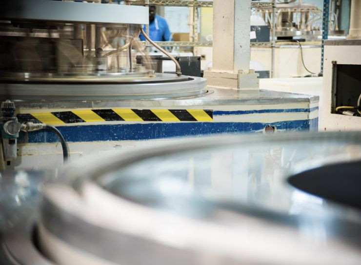
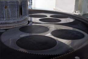
Double Side Lapping
Our primary means of surface grinding, double-side lapping produces far superior thickness, flatness, and parallelism results than the typical single-side process. Coresix has a long history and extensive experience in machine conditioning and process design to achieve what others cannot. Our 20" platforms can accommodate parts as large as 450mm and as thin as 450um.
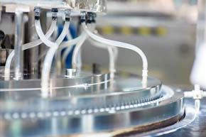
Glass Thinning
For wafer applications requiring characteristics not available in the raw glass form including thickness, thickness tolerance, thickness variation, flatness, and parallelism, these critical specifications are established early in the fabrication process through double-side lapping. We run multiple platforms and variations of the lapping process to consistently meet the most stringent of these requirements from small volume R&D to high volume production.
Common Flatness Terms
Flatness
Of a surface is the degree to which the surface approximates a mathematical plane. Flatness is typically specified in microns, waves, or fringes (half waves).
Bow
The deviation of the center point of the median surface of a free, unclamped wafer from the median surface reference plane is established by three points equally spaced on a circle with a diameter of a specified amount less than the nominal diameter of the wafer. Bow is typically measured in microns.
TTV
Total Thickness Variation – expresses the maximum peak to valley measurement within a given part or from one part to the next.
Warp
The difference between the maximum and minimum distances of the median surface of a free, unclamped wafer from a reference place.
Lapping Capabilities
| Lapping | Minimum | Maximun | Tolerance |
|---|---|---|---|
| Flatness | 1/10 Wave | n/a | n/a |
| Bow/Warp | <1um/Inch | n/a | n/a |
| TTV | NA +/-1um | ||
| Thickness | 200um | n/a | +/-5um |
| Size | 10mm | 300mm | +/-0.10mm |